The Square Revolution: Why the Semiconductor Industry is Shifting to Fan-Out Panel-Level Packaging (FOPLP)
ASX 0.00%↑
GOOGL 0.00%↑
AMD 0.00%↑
NVDA 0.00%↑
TSM 0.00%↑
The semiconductor industry is going through a major shape change. It is pivoting from the round geometry of silicon wafers to the rectangular efficiency of panels. Artificial intelligence (AI) and high-performance computing (HPC) now demand chips with incredible power and size. The physical limits of older manufacturing methods are forcing a move toward Fan-Out Panel-Level Packaging (FOPLP). This shift changes both material science and economic output. It is driven by the need to combine different “chiplets” and high-bandwidth memory (HBM) into single, massive packages that exceed what legacy systems can handle.
The Traditional Bottleneck: Wafer-Level Packaging
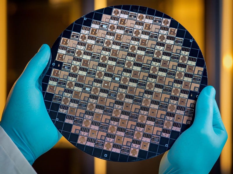
To understand this shift, one must first look at the current standard. This includes Fan-Out Wafer-Level Packaging (FOWLP) and 2.5D technologies like TSMC’s Chip-on-Wafer-on-Substrate (CoWoS). Traditionally, makers package chips on 300mm circular silicon wafers. This method is mature and precise, but it faces two critical problems in the AI era.
First is the “reticle limit.” Lithography tools can only pattern a specific maximum area in a single exposure, which is roughly 26mm x 33mm. Technologies like CoWoS-L use silicon bridges to stitch parts together, but the physical size of the 300mm wafer still limits them. Second is geometric waste. Placing square or rectangular chips onto a round wafer leaves unused space at the edges. A 300mm wafer typically reaches only about 85% area utilization. This limits the number of chips that can be processed at once. As AI processors like Nvidia’s Blackwell grow larger, the number of units per wafer drops. This drives up costs and creates supply bottlenecks.
The Switch to FOPLP: Efficiency in Geometry
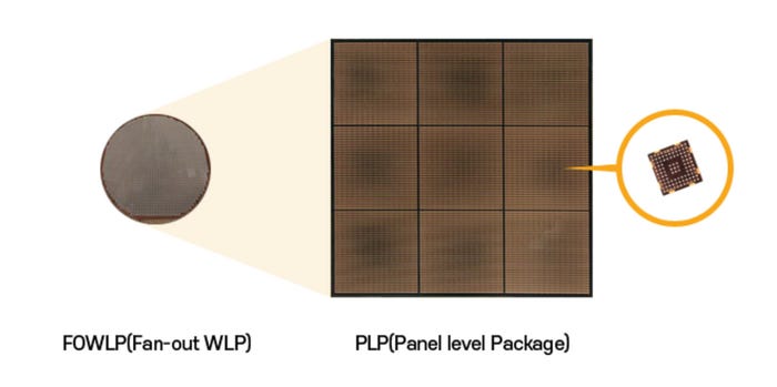
FOPLP fixes these issues by moving from “circles to squares.” By using large rectangular panels made of glass or organic laminates, manufacturers can push carrier utilization to over 95%.
The economic reasons are strong. Switching to panel formats can cut packaging costs by more than 20% because of higher throughput. A 600mm x 600mm panel offers approximately 5.09 times the usable area of a standard 300mm wafer. A 700mm x 700mm panel offers nearly 7 times the capacity. This scale allows for the integration of larger Systems-in-Package (SiP) needed for yotta-scale computing. It effectively bypasses the size constraints of silicon interposers.
ASE Technology: Leading the Standardization Charge
ASE Technology Holding is leading this transition. They are the world’s largest Outsourced Semiconductor Assembly and Test (OSAT) provider. ASE has positioned its Fan-Out Chip-on-Substrate (FOCoS) platform to bridge the gap between cost-effective organic substrates and high-performance silicon interposers.
ASE’s most advanced technique in this area is the FOCoS-Bridge. This architecture embeds tiny silicon bridges within an organic interposer. It provides ultra-fine routing (Line/Space < 0.5µm) only where needed, specifically between logic dies and memory. It uses standard routing everywhere else. This mix lowers the high costs of using massive silicon interposers while keeping the bandwidth necessary for AI workloads.
ASE is not working alone. The company has aligned strategically with TSMC to co-develop industry standards for panel sizes. Currently, the partners are focusing on a 310mm x 310mm panel flow. This standardization is vital. By agreeing on a form factor, ASE and TSMC can pool capital expenditures, learn faster, and create a unified ecosystem for equipment vendors. This size serves as a stepping stone. It allows engineers to refine pick-and-place precision and lithography tools before scaling to the harder 600mm x 600mm format. ASE has raised its 2025 capital expenditure to nearly $6 billion to support these expansions, showing high confidence in a panel-level future.
Big Tech Adopters: Vertical Integration and Custom Silicon
Major technology firms are driving the migration to FOPLP to control their own supply chains and reduce reliance on traditional bottlenecks.
SpaceX
Perhaps the most aggressive new player in FOPLP is SpaceX. The aerospace giant is building its own advanced chip packaging factory in Bastrop, Texas. This project is supported by a $17.3 million grant from the Texas Semiconductor Innovation Fund. SpaceX is targeting a substrate size of 700mm x 700mm, which is purported to be the largest in the industry.
This move is a play for vertical integration. Starlink satellites and user terminals require millions of chips annually. By bringing packaging in-house, SpaceX aims to compress its supply chain, cut costs, and secure domestic production for critical RF components. The facility benefits from synergies with SpaceX’s existing Printed Circuit Board (PCB) manufacturing at the same site, as FOPLP processes share similarities with advanced PCB fabrication.
Google has utilized FOPLP to optimize costs for its consumer devices. The Tensor G4 processor, powering the Pixel 9 series, utilized Samsung’s FOPLP technology. Reports indicate Google may switch to TSMC’s wafer-level InFO packaging for the Tensor G5 to maximize performance and power efficiency. However, the use of FOPLP for the G4 demonstrates the technology is viable for high-volume mobile processors where cost-efficiency is key.
AMD
AMD is pivoting aggressively toward panel-level and glass substrates for its future high-performance plans. For its Instinct MI500 series, slated for 2027, AMD is exploring glass substrates. This would facilitate the massive interconnect density required for “yotta-scale” computing. AMD has secured patents for bonding glass substrates and is actively evaluating samples from supply partners like Absolics. They want to ensure they can deliver the 1,000x performance increase targeted for their next-generation AI accelerators.
Other Key Players and the Ecosystem
The FOPLP ecosystem is expanding quickly and involves foundries, OSATs, and material suppliers.
Nvidia is the dominant force in AI and the primary driver for TSMC’s roadmap. TSMC is developing CoPoS (Chip-on-Panel-on-Substrate) specifically to meet the needs of Nvidia’s future Rubin architecture. This architecture will require interposers larger than what 300mm wafers can provide.
Samsung Electronics is a pioneer in the field. They acquired the PLP business from their electro-mechanics division in 2019. Samsung is advancing its “H-glass” roadmap and has applied FOPLP to wearable processors like the Exynos W920.
Intel is a leader in next-generation materials. They have moved their glass substrate production in Arizona into high-volume manufacturing for their Xeon 6 “Clearwater Forest” processors. Intel positions glass as the successor to organic panels.
STMicroelectronics is celebrating a decade-long partnership with SpaceX. They developed a proprietary PLP manufacturing process to deliver over 5 million chips per day for Starlink terminals. This proves the technology is capable of high-volume RF applications.
Powertech Technology Inc. (PTI), a Taiwan-based OSAT, is investing NT$43.3 billion to accelerate FOPLP. They are targeting mass production in 2027.
Equipment and material suppliers are also involved. Companies like Onto Innovation are providing critical lithography and defect inspection tools for large panels. Absolics, a subsidiary of SKC, has opened a $600 million facility in Georgia to supply glass substrates to customers like AMD. E&R Engineering is delivering laser and plasma solutions essential for drilling Through-Glass Vias (TGV).
The industry shift to FOPLP is not just an upgrade. It is a necessity. As the physical limits of the “circle” are reached, the “square” panel offers the surface area, cost structure, and heterogeneous integration capabilities required to power the next generation of artificial intelligence and global connectivity.
Disclaimer:
All views expressed are my own and are provided solely for informational and educational purposes. This is not investment, legal, tax, or accounting advice, nor a recommendation to buy or sell any security. While I aim for accuracy, I cannot guarantee completeness or timeliness of information. The strategies and securities discussed may not suit every investor; past performance does not predict future results, and all investments carry risk, including loss of principal.
I may hold, or have held, positions in any mentioned securities. Opinions herein are subject to change without notice. This material reflects my personal views and does not represent those of any employer or affiliated organization. Please conduct your own research and consult a licensed professional before making any investment decisions.


